| CPC H01L 23/10 (2013.01) [H01L 23/04 (2013.01); H01L 23/053 (2013.01); H01L 24/73 (2013.01); H01L 25/072 (2013.01); H01L 25/18 (2013.01); H01L 2224/73265 (2013.01); H01L 2924/1033 (2013.01); H01L 2924/10254 (2013.01); H01L 2924/10272 (2013.01)] | 19 Claims |
|
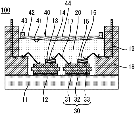
1. A semiconductor device comprising:
a base plate;
a case that surrounds a region immediately above the base plate in plan view;
a semiconductor chip provided in the region;
a sealing resin that fills the region; and
a barrier layer provided on the sealing resin,
wherein the barrier layer has
a first surface facing the base plate,
a second surface opposite to the first surface, and
a convex part protruding upward from the second surface,
the first surface has the shortest distance to the base plate at a center of the barrier layer and has a continuously longer distance to the base plate as getting farther from the center,
the convex part is provided at least on each of both sides of the center, while avoiding the center, and
a height of the convex part from the second surface is greater than a distance in a thickness direction of the barrier layer between a portion of the first surface immediately below the convex part and a portion of the first surface provided at the center.
|