| CPC H01L 22/10 (2013.01) [G01M 11/30 (2013.01); G02B 6/13 (2013.01); H01L 31/02325 (2013.01); H01L 31/1808 (2013.01)] | 9 Claims |
|
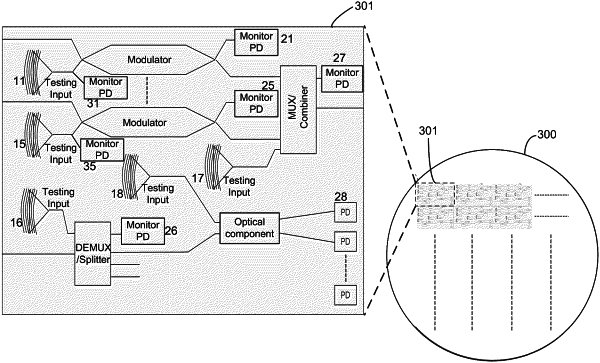
1. A silicon photonics integrated circuit comprising:
a plurality of optical devices, ones of the optical devices including inputs and outputs configured for use during normal operation and additionally including test inputs and test outputs configured for use during testing;
optical couplers coupled to the test inputs of the optical devices, the optical couplers configured to couple optical test signals to the test inputs during the testing of the optical devices to test optical characteristics of the optical devices, wherein the optical characteristics of the optical devices comprise one or more of temporal, magnitude, and frequency characteristics of signals at one or more of the inputs and outputs of the optical devices; and
photodetectors coupled to the test outputs of the optical devices, the photodetectors configured to detect output signals at the test outputs, the output signals including responses of the optical devices to the optical test signals during the testing of the optical devices, the output signals being indicative of the optical characteristics of the optical devices.
|