| CPC H01L 21/82385 (2013.01) [H01L 21/28088 (2013.01); H01L 21/32134 (2013.01); H01L 21/823821 (2013.01); H01L 27/0924 (2013.01); H01L 29/4966 (2013.01); H01L 29/66545 (2013.01); H01L 29/66795 (2013.01); H01L 29/7851 (2013.01)] | 20 Claims |
|
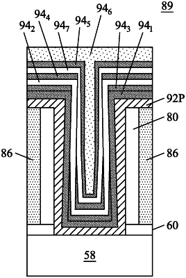
1. A device comprising:
a gate stack over an active region of a substrate, the gate stack comprising:
a conductive material;
a first protective layer lining sidewalls and a bottom surface of the conductive material;
a second protective layer lining sidewalls and a bottom surface of the first protective layer, the first protective layer and the second protective layer comprising different materials;
an N-type work function layer lining sidewalls and a bottom surface of the second protective layer, an upper portion of the N-type work function layer being in physical contact with an upper portion of the first protective layer;
a gate dielectric layer lining sidewalls and a bottom surface of the N-type work function layer;
a P-type work function layer between the N-type work function layer and the gate dielectric layer; and
a third protective layer between the N-type work function layer and the P-type work function layer, the upper portion of the N-type work function layer being in physical contact with an upper portion of the P-type work function layer.
|