| CPC H01L 21/67259 (2013.01) [H01L 21/6833 (2013.01); H01L 22/14 (2013.01); H02N 13/00 (2013.01)] | 15 Claims |
|
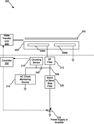
1. A wafer chucking monitor comprising:
a voltage source configured to provide a voltage to a wafer chuck;
an AC source configured to provide an AC monitoring signal to the wafer chuck via a node between the wafer chuck and the voltage source;
a blocking capacitor arranged between the AC source and the node;
a chucking sensor arranged between the blocking capacitor and the AC source and configured to monitor current and voltage on a low voltage side of the blocking capacitor;
a filter arranged between the node and the voltage source; and
a controller configured to receive the current and voltage from the chucking sensor and ascertain a chucking state.
|