| CPC H01L 21/02381 (2013.01) [H01J 37/32449 (2013.01); H01L 21/0234 (2013.01); H01L 21/02532 (2013.01); H01L 21/3065 (2013.01); H01L 21/30655 (2013.01); H01L 21/31116 (2013.01); H01L 21/31144 (2013.01); H01L 21/32135 (2013.01); H01L 21/32136 (2013.01); H01L 21/32137 (2013.01); H01J 2237/3341 (2013.01)] | 20 Claims |
|
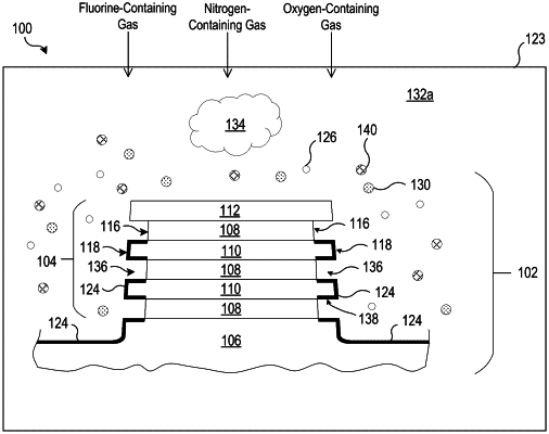
1. A method of processing a semiconductor substrate, the method comprising:
receiving a semiconductor substrate that comprises a film stack, the film stack comprising a first germanium-containing layer, a second germanium-containing layer, and a first silicon layer positioned between the first germanium-containing layer and the second germanium-containing layer;
in a first plasma step, generating a first plasma and modifying exposed surfaces of the first germanium-containing layer, the second germanium-containing layer, and the first silicon layer by exposing the exposed surfaces to the first plasma, modifying the exposed surfaces including:
removing at least a portion of a native oxide layer from the exposed surfaces of the first silicon layer; and
forming a passivation layer on the exposed surfaces of the first germanium-containing layer and the second germanium-containing layer; and
in a second plasma step, generating a second plasma and etching, using the second plasma, the first silicon layer to form an indent in the film stack at the first silicon layer between the first germanium-containing layer and the second germanium-containing layer, the passivation layer inhibiting etching of the first germanium-containing layer and the second germanium-containing layer, the second plasma being different than the first plasma.
|