| CPC H01L 29/78609 (2013.01) [G06K 19/07758 (2013.01); H01L 21/8236 (2013.01); H01L 23/66 (2013.01); H01L 27/0883 (2013.01); H01L 27/1225 (2013.01); H01L 29/24 (2013.01); H01L 29/26 (2013.01); H01L 29/66969 (2013.01); H01L 29/7869 (2013.01); H01L 29/78696 (2013.01); G11C 7/00 (2013.01); G11C 19/28 (2013.01); H01L 2223/6677 (2013.01); H02M 3/07 (2013.01)] | 6 Claims |
|
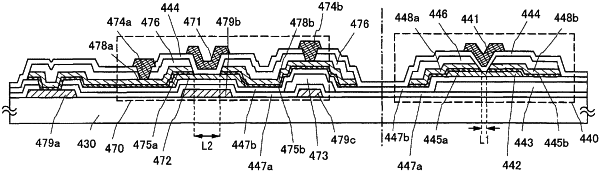
1. A semiconductor device comprising:
a first transistor over a glass substrate, the first transistor comprising a first oxide semiconductor layer where a channel formation region is provided,
a second transistor over the glass substrate, the second transistor comprising a second oxide semiconductor layer where a channel formation region is provided,
wherein each of the first oxide semiconductor layer and the second oxide semiconductor layer comprises indium and zinc,
wherein a conductive layer is provided between the substrate and the first oxide semiconductor layer,
wherein a first insulating layer is provided between the conductive layer and the first oxide semiconductor layer,
wherein each of the first oxide semiconductor layer and the second oxide semiconductor layer are over and in direct contact with the first insulating layer,
wherein a channel length of the first transistor is longer than a channel length of the second transistor,
wherein no conductive layer is provided between the substrate and the second oxide semiconductor layer, and
wherein a size of crystal grains in each of the first oxide semiconductor layer and the second oxide semiconductor layer is greater than or equal to 1 nm and smaller than or equal to 20 nm.
|