| CPC H01L 21/76224 (2013.01) [H01L 21/0337 (2013.01); H01L 21/28247 (2013.01); H01L 21/28568 (2013.01); H01L 21/3086 (2013.01); H01L 21/31105 (2013.01); H01L 21/31144 (2013.01); H01L 21/76816 (2013.01); H01L 21/823431 (2013.01); H01L 21/823481 (2013.01); H01L 21/823807 (2013.01); H01L 21/823814 (2013.01); H01L 21/823821 (2013.01); H01L 21/823842 (2013.01); H01L 21/823857 (2013.01); H01L 21/823871 (2013.01); H01L 21/823878 (2013.01); H01L 23/5226 (2013.01); H01L 23/5283 (2013.01); H01L 23/53238 (2013.01); H01L 23/53266 (2013.01); H01L 27/0886 (2013.01); H01L 27/0924 (2013.01); H01L 28/24 (2013.01); H01L 29/0847 (2013.01); H01L 29/516 (2013.01); H01L 29/6653 (2013.01); H01L 29/66795 (2013.01); H01L 29/66818 (2013.01); H01L 29/785 (2013.01); H01L 29/7843 (2013.01); H01L 29/7846 (2013.01); H01L 29/7848 (2013.01); H01L 29/7854 (2013.01); H10B 10/12 (2023.02)] | 20 Claims |

|
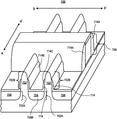
1. A method of fabricating an integrated circuit structure, the method comprising:
forming a fin comprising silicon, the fin having a lower fin portion and an upper fin portion;
forming an insulating structure directly adjacent sidewalls of the lower fin portion of the fin;
forming first and second gate structures over the upper fin portion and over first and second portions of the insulating structure, respectively;
forming a dielectric material conformal with the upper fin portion of the fin, conformal with the first and second gate structures, and conformal with a third portion of the insulating structure between the first gate structure and the second gate structure;
forming a hardmask material over the dielectric material;
recessing the hardmask material to expose a portion of the dielectric material conformal with the upper fin portion of the fin and conformal with the first and second gate structures, the recessed hardmask material covering a portion of the dielectric material conformal with the third portion of the insulating structure between the first gate structure and the second gate structure; and
anisotropically etching the dielectric material and subsequently removing the recessed hardmask material to form a first dielectric spacer along a sidewall of the first gate structure and a second dielectric spacer along a sidewall of the second gate structure, the second dielectric spacer continuous with the first dielectric spacer over the third portion of the insulating structure between the first gate structure and the second gate structure.
|