| CPC H01G 4/1227 (2013.01) [C04B 35/06 (2013.01); C04B 35/4682 (2013.01); H01G 4/008 (2013.01); H01G 4/012 (2013.01); H01G 4/30 (2013.01); C04B 2235/658 (2013.01)] | 15 Claims |
|
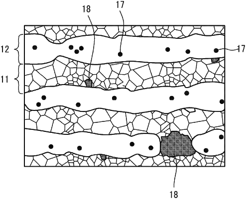
1. A ceramic electronic device comprising:
a plurality of dielectric layers of which a main component is a ceramic having a perovskite structure; and
a plurality of internal electrode layers, each of which is alternatively stacked with each of the plurality of dielectric layers and includes metal crystal grains, and a co-material which is inactive against the main component of the plurality of dielectric layers, without including a ceramic having a same composition as the ceramic of the main component of the plurality of dielectric layers.
|