| CPC G11C 29/42 (2013.01) [G11C 16/102 (2013.01); G11C 16/26 (2013.01); G11C 29/12005 (2013.01); G11C 29/44 (2013.01)] | 20 Claims |
|
1. A system comprising:
a memory device; and
a processing device, operatively coupled to the memory device, to perform operations comprising:
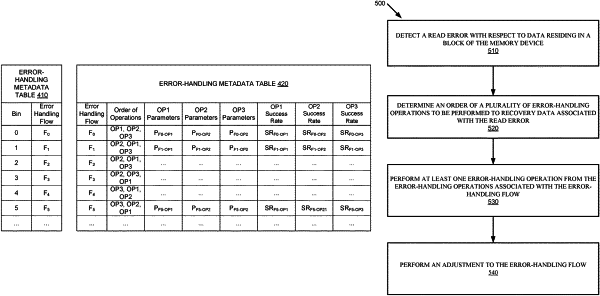
selecting, from a plurality of voltage offset bins, a voltage offset bin associated with a block of the memory device, wherein each voltage offset bin corresponds to a respective predetermined range of threshold voltage offsets to be applied to a base voltage read level during read operations;
performing, on data residing in the block, an error-handling operation of a plurality of error-handling operations, wherein an order of the plurality of error-handling operations is based on the voltage offset bin associated with the block; and
responsive to determining that the error-handling operation has failed to recover the data, adjusting the order of the plurality of error-handling operations.
|