US 11,837,291 B2
Voltage offset bin selection by die group for memory devices
Vamsi Pavan Rayaprolu, San Jose, CA (US); Mustafa N. Kaynak, San Deigo, CA (US); Michael Sheperek, Longmont, CO (US); Larry J. Koudele, Erie, ID (US); and Shane Nowell, Boise, ID (US)
Assigned to Micron Technology, Inc., Boise, ID (US)
Filed by Micron Technology, Inc., Boise, ID (US)
Filed on Jan. 31, 2022, as Appl. No. 17/589,491.
Application 17/589,491 is a continuation of application No. 17/008,225, filed on Aug. 31, 2020, granted, now 11,270,772.
Prior Publication US 2022/0157385 A1, May 19, 2022
This patent is subject to a terminal disclaimer.
Int. Cl. G11C 16/10 (2006.01); G06F 12/06 (2006.01); G11C 16/08 (2006.01)
CPC G11C 16/107 (2013.01) [G06F 12/06 (2013.01); G11C 16/08 (2013.01)] 20 Claims
OG exemplary drawing
 
1. A system comprising:
a memory device; and
a processing device, operatively coupled to the memory device, to perform operations comprising:
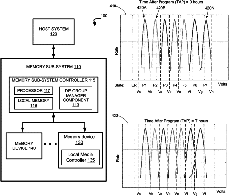
programming, at the memory device, one or more data units that are associated with one or more dice of a die group comprising a plurality of dice; and
determining, based on a subset of dice of the die group, a voltage offset bin associated with the plurality of dice in the die group, wherein the voltage offset bin identifies a set of read level offsets associated with performing a read operation at the memory device.