| CPC G11C 13/0069 (2013.01) [G11C 13/004 (2013.01); G11C 13/0026 (2013.01); G11C 13/0028 (2013.01); G11C 13/0038 (2013.01)] | 18 Claims |
|
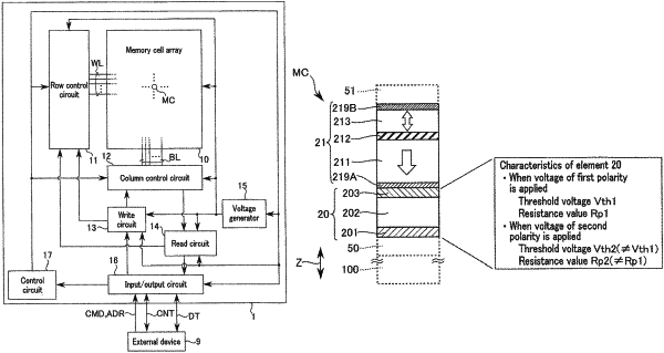
1. A memory device comprising:
a memory cell including a memory element and a switching element; and
a circuit that applies a first write pulse having a first polarity to the memory cell at the time of writing first data in the memory cell and applies a second write pulse having a second polarity different from the first polarity to the memory cell at the time of writing second data in the memory cell,
wherein
the switching element has polarity dependence according to the first and second polarities.
|