| CPC G11C 13/003 (2013.01) [G11C 13/0026 (2013.01); G11C 13/0028 (2013.01); G11C 13/0004 (2013.01); G11C 13/0011 (2013.01)] | 26 Claims |

|
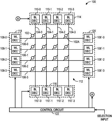
1. A memory device, comprising:
a plurality of wordlines;
a plurality of bitlines, wherein the plurality of wordlines and the plurality of bitlines form a grid;
a plurality of memory cells located at intersections of the plurality of bitlines and the plurality of wordlines in the grid;
a plurality of bitline drivers;
a plurality of wordline drivers; and
compensation circuitry configured to:
determine a bitline distance of a first bitline driver of the plurality of bitline drivers from a first memory cell of the plurality of memory cells, a wordline distance of a first wordline driver of the plurality of wordline drivers from the first memory cell, or both the wordline distance and the bitline distance; and
output values to control one or more voltages applied to the first memory cell based at least in part on the bitline distance, the wordline distance, or both.
|