| CPC G11C 11/5635 (2013.01) [G11C 5/145 (2013.01); G11C 11/5642 (2013.01); G11C 16/06 (2013.01); G11C 16/08 (2013.01); H03K 17/102 (2013.01)] | 20 Claims |

|
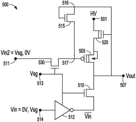
1. An electronic device comprising:
a switch circuit structured as a high-voltage switch circuit in the electronic device, the switch circuit comprising:
a transistor having a first gate separated from a channel structure by a dielectric region, the transistor coupled to receive a voltage from a node of the switch circuit, the voltage being a high voltage for the electronic device;
an output node coupled to the transistor, with the output node coupled to transfer the voltage from the transistor externally from the switch circuit;
a diode structure coupled to the output node and to the first gate, the diode structure being a feedback structure arranged to provide feedback to the transistor from the output node; and
control circuitry structured to control timing of an input signal to the transistor such that voltage across the dielectric region is operatively prevented from entering a Fowler-Nordheim regime.
|