| CPC G11C 11/4094 (2013.01) [G11C 11/406 (2013.01); G11C 11/4091 (2013.01); G11C 11/4096 (2013.01)] | 20 Claims |
|
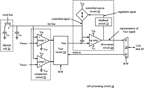
10. A cell processing circuit of a Dynamic Random Access (DRAM) memory device, the cell processing circuit comprises:
a read-write circuit operably coupled to a bit-line of a DRAM memory device, wherein the read-write circuit is configured to drive the bit-line at a first voltage for pre-charging a parasitic capacitance between a ground and the bit-line to a second voltage, wherein the second voltage is between a logic 1 voltage and a logic 0 voltage, wherein the bit-line is operably coupled to a plurality of DRAM cells including a first DRAM cell of the DRAM memory device;
a drive sense circuit operably coupled to the bit line, wherein the drive sense circuit is operable to sense a voltage change on the bit-line when the parasitic capacitance is coupled in parallel to a DRAM cell capacitor of the first DRAM cell; and
an input selection circuit operably coupled to the drive sense circuit and operably coupled to the read-write circuit, wherein the read-write circuit is configured to receive an output from the input selection circuit and generate a read output voltage based on the output from the input selection circuit, wherein the read-write circuit is further configured to apply the read output voltage to the bit-line to refresh a voltage stored by the first DRAM cell.
|