| CPC G11C 11/2273 (2013.01) [G11C 11/221 (2013.01); G11C 11/2259 (2013.01); G11C 11/2275 (2013.01); G11C 11/4091 (2013.01); G11C 11/4096 (2013.01)] | 25 Claims |

|
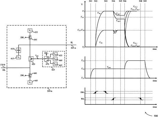
1. An apparatus, comprising:
a memory cell operable to couple with a first portion of an access line;
a sense component operable to couple with a second portion of the access line;
a transistor having a channel portion between the first portion of the access line and the second portion of the access line; and
circuitry operable to:
bias a gate portion of the transistor with a first voltage for isolating the first portion of the access line from the second portion of the access line;
bias the gate portion of the transistor with a second voltage for coupling the first portion of the access line with the second portion of the access line during a read operation on the memory cell wherein, while biasing the gate portion of the transistor with the second voltage during the read operation, charge flows between the second portion of the access line and the first portion of the access line across the transistor until a voltage of the first portion of the access line is within a threshold difference of the second voltage; and
bias the gate portion of the transistor with a third voltage, greater than the second voltage, for coupling the first portion of the access line with the second portion of the access line during a write operation on the memory cell.
|