| CPC G09G 3/3233 (2013.01) [G09G 3/3258 (2013.01); G09G 3/3283 (2013.01); G09G 3/3291 (2013.01); G09G 2310/0262 (2013.01); G09G 2320/0214 (2013.01); G09G 2320/0233 (2013.01); G09G 2320/0257 (2013.01); G09G 2320/0295 (2013.01); G09G 2320/045 (2013.01); G09G 2320/0626 (2013.01); G09G 2330/026 (2013.01); H10K 50/30 (2023.02)] | 13 Claims |
|
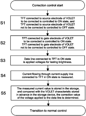
1. A method of compensating brightness of a display comprising a plurality of vertical organic light emitting transistors and a memory element that stores characteristic information about vertical organic light emitting transistor performance characteristics, the method comprising:
a step (A) of applying a voltage for brightness inspection to a gate electrode of a vertical organic light emitting transistor to be corrected;
a step (B) of measuring a current flowing through a current supply line through which the current is supplied to a source electrode of the vertical organic light emitting transistor by the application of the voltage for brightness inspection to the gate electrode of the vertical organic light emitting transistor to be corrected; and
a step (C) of determining a corrected value of the voltage to be applied to the gate electrode of the vertical organic light emitting transistor based on a value of the current measured in the step (B) and the characteristic information of the vertical organic light emitting transistor stored in the memory element,
wherein the step (A) comprises a step (A1) of cutting off supply of a current to vertical organic light emitting transistors not to be corrected.
|