| CPC G09G 3/32 (2013.01) [G09G 2300/0842 (2013.01); G09G 2310/0216 (2013.01); G09G 2310/0286 (2013.01)] | 26 Claims |
|
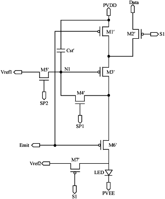
1. A pixel circuit, comprising:
a drive circuit, wherein a control terminal of the drive circuit is electrically connected to a first node, a first terminal of the drive circuit is electrically connected to a second node, and a second terminal of the drive circuit is electrically connected to a third node;
a first initialization circuit, wherein a first terminal of the first initialization circuit is electrically connected to a first reference signal terminal, and a second terminal of the first initialization circuit is electrically connected to the third node;
a data write circuit, wherein a control terminal of the data write circuit is electrically connected to a scanning signal terminal, a first terminal of the data write circuit is electrically connected to a data signal terminal, and a second terminal of the data write circuit is electrically connected to the second node; and
a threshold compensation circuit, wherein a control terminal of the threshold compensation circuit is electrically connected to an enable signal terminal, a first terminal of the threshold compensation circuit is electrically connected to the third node, and a second terminal of the threshold compensation circuit is electrically connected to the first node.
|