| CPC G06V 40/1306 (2022.01) | 5 Claims |
|
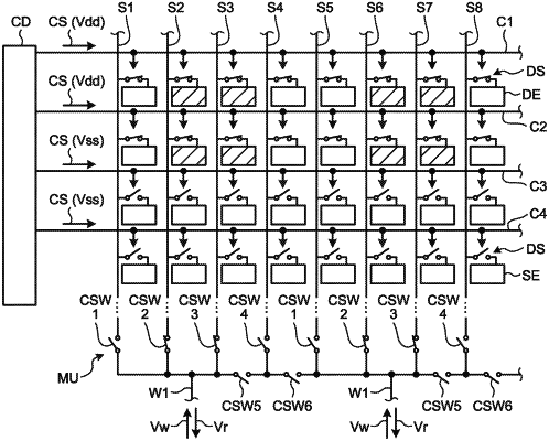
1. A fingerprint sensor comprising: a substrate;
a plurality of sensor electrodes arranged on the substrate;
a plurality of first switches coupled to the sensor electrodes; an organic layer covering the sensor electrodes;
a control line drive circuit that is provided and long in a first direction;
a signal line drive circuit that is provided and long in a second direction orthogonal to the first direction;
a plurality of signal lines coupled to the first switches;
a plurality of control lines coupling the first switches to the control line drive circuit; a sensor drive electrode surrounding the sensor electrodes;
a plurality of second switches that are provided between the signal line drive circuit and the signal lines and in a one-to-one correspondence with the signal lines; and
a first number of third switches that are provided between the signal line drive circuit and the first number of second switches of all the second switches and in a one-to-one correspondence with the first number of second switches,
wherein a position of a surface of the organic layer is lower than a position of the sensor drive electrode, and
wherein the first number is less than the number of all the second switches.
|