| CPC G06F 3/0655 (2013.01) [G06F 3/0604 (2013.01); G06F 3/0679 (2013.01)] | 20 Claims |
|
1. A system comprising:
a memory device; and
a processing device, operatively coupled with the memory device, the processing device configured to perform operations comprising:
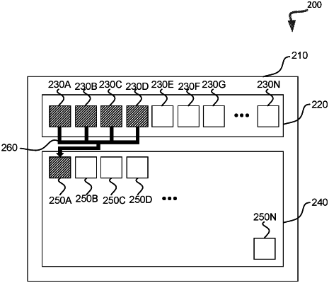
determining whether a subset of write units of a primary region of the memory device corresponding to a pre-determined number of write units of the primary region is written with data received from a host system;
determining that at least one write unit in the subset of write units of the primary region stores invalid data; and
in response to determining that the subset of write units of the primary region corresponding to the pre-determined number of write units is written, performing a write operation on at least one write unit of a secondary region of the memory device with respective data of the subset of write units of the primary region, the respective data comprising the invalid data.
|