| CPC G06F 21/74 (2013.01) [G06F 2221/2123 (2013.01)] | 20 Claims |
|
1. A secure semiconductor chip, comprising:
a logic layer that comprises access logic and a logic circuit formed within the logic layer;
a first memory layer comprising non-volatile resistive memory cells disposed over the logic layer and integrated with the logic layer in a monolithic structure embodying the secure semiconductor chip; and
a plurality of connectors within vias provided between the logic layer and the first memory layer facilitating intra-chip communication within an interior of the secure semiconductor chip; wherein:
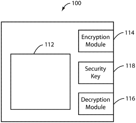
the access logic is configured to receive a security key stored in non-volatile resistive memory cells of the first memory layer by way of the plurality of connectors, and
the access logic is configured to provide access to the logic circuit formed within the logic layer in response to successfully receiving the security key.
|