| CPC G03F 7/0002 (2013.01) [H01L 21/0271 (2013.01)] | 2 Claims |
|
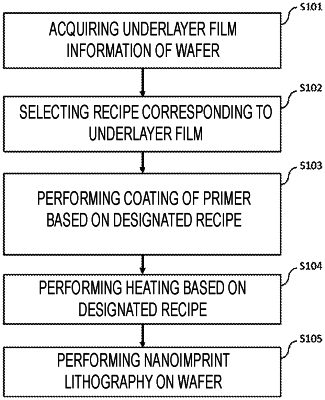
1. A semiconductor device manufacturing method performed by an imprint device including a sensor configured to read, from a semiconductor substrate, information indicating both a thickness of a film on the substrate and a type of the film, the method comprising:
loading a semiconductor substrate on which a first film has been formed onto a load port of the imprint device;
acquiring information about the first film by controlling the sensor to read symbols on the semiconductor substrate, the information indicating both the thickness of the first film that has been formed on the substrate and the type of the first film;
selecting a recipe for primer processing conditions corresponding to the acquired information about the first film;
conveying the semiconductor substrate on the load port to a stage of the imprint device;
forming a primer layer on the semiconductor substrate by coating of a primer on the semiconductor substrate on the stage according to the recipe;
conveying the semiconductor substrate from the stage to a first chamber of the imprint device;
heating the semiconductor substrate after the forming of the primer layer, the heating being performed in the first chamber according to the recipe;
conveying the semiconductor substrate from the first chamber to a second chamber of the imprint device;
patterning a resist dispensed onto the semiconductor substrate using imprint lithography in the second chamber; and
processing the first film by using the patterned resist on the semiconductor substrate as a mask.
|