| CPC G02F 1/136286 (2013.01) [G02F 1/1368 (2013.01); G02F 1/136209 (2013.01)] | 20 Claims |
|
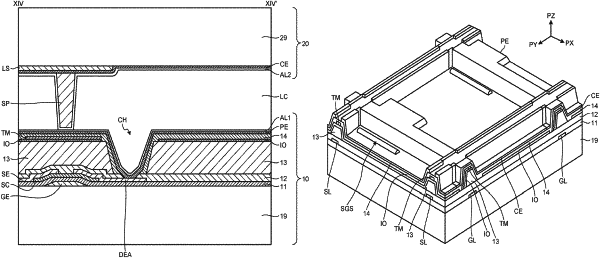
1. A display panel comprising:
an array substrate including:
a plurality of pixels arranged in a matrix having a row-column configuration in a display region,
an organic insulating layer,
a first inorganic insulating layer covering the organic insulating layer,
a first light-transmitting electrode between the organic insulating layer and the first inorganic insulating layer, and
a metal layer between the organic insulating layer and the first inorganic insulating layer and having a first grid shape in the display region;
a counter substrate; and
a liquid crystal layer including polymer-dispersed liquid crystals and disposed between the array substrate and the counter substrate,
wherein
the organic insulating layer has a second grid shape in the display region,
the first light-transmitting electrode has a third grid shape in the display region,
the organic insulating layer having the second grid shape overlaps the first light-transmitting electrode having the third grid shape,
the first light-transmitting electrode having the third grid shape (1) overlaps the metal layer that has the first grid shape and (2) contains a plurality of openings defined by the third grid shape and surrounded by the first grid shape of the metal layer, and
the metal layer having the first grid shape is in contact with the first light-transmitting electrode that has the third grid shape.
|