| CPC G02B 6/122 (2013.01) [G02B 6/12007 (2013.01); G02B 2006/12104 (2013.01); G02B 2006/12164 (2013.01)] | 18 Claims |
|
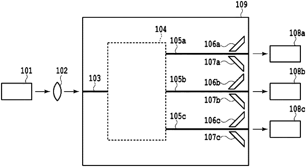
1. A planar optical waveguide circuit having an optical waveguide embedded in a cladding layer, the planar optical waveguide circuit comprising:
a plurality of parallel output optical waveguides configured to emit light from a same end face; and
a groove formed in the cladding layer, the groove having a reflective interface configured to reflect leaked light propagating in the cladding layer,
wherein:
the reflective interface includes a reflective interface formed at an angle of +45 degrees and a reflective interface formed at an angle of −45 degrees relative to the output optical waveguides,
the reflective interface formed at an angle of +45 degrees, the output optical waveguide, and the reflective interface formed at −45 degrees being arranged repeatedly in that order.
|