| CPC G02B 6/12007 (2013.01) [G02B 6/125 (2013.01); G02B 6/29338 (2013.01)] | 13 Claims |
|
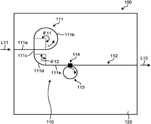
1. An optical waveguide circuit comprising:
a ring waveguide;
an input connection waveguide;
an output connection waveguide; and
an optical multiplexing/demultiplexing part that optically connects the ring waveguide with the input connection waveguide, and that optically connects the ring waveguide with the output connection waveguide, wherein
at least one of the input connection waveguide and the output connection waveguide includes a plurality of curved waveguides,
a sum total of products of curvature signs and bending angles of the curved waveguides and a sum total of a curvature sign and a bending angle of the ring waveguide have a same absolute value with signs opposite to each other, and
rotation of a polarization plane of light generated in the ring waveguide and rotation of a polarization plane of light generated in the curved waveguides cancel each other out.
|