| CPC G01R 31/3171 (2013.01) [G06F 11/076 (2013.01); G06F 11/0745 (2013.01); G06F 11/0793 (2013.01)] | 20 Claims |
|
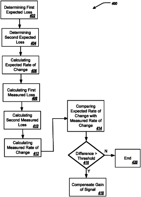
1. A method of compensating for signal loss, the method comprising:
determining a first expected loss at a first frequency at a receiver associated with a first lane of a printed circuit board (PCB);
determining a second expected loss at a second frequency at the receiver associated with the first lane of the PCB;
calculating an expected rate of change of signal loss between the first frequency and the second frequency based on the first expected loss and the second expected loss;
calculating a first measured loss of a first signal transmitted at the first frequency from a transmitter to the receiver along the first lane of the PCB;
calculating a second measured loss of a second signal transmitted at the second frequency from the transmitter to the receiver along the first lane of the PCB;
calculating a measured rate of change of signal loss between the first frequency and the second frequency based on the first measured loss and the second measured loss;
comparing the measured rate of change of signal loss with the expected rate of change of signal loss; and
compensating, based on the comparison, a gain of a particular signal transmitted from the transmitter to the receiver.
|