| CPC H10K 71/00 (2023.02) [H10K 50/135 (2023.02); H10K 50/15 (2023.02); H10K 50/16 (2023.02); H10K 59/122 (2023.02); H10K 71/221 (2023.02); H10K 59/1201 (2023.02)] | 10 Claims |
|
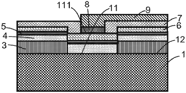
1. A manufacturing method of an optoelectronic device, wherein a characteristic size of a single light-emitting pixel or effective working region of the optoelectronic device is less than or equal to 500 microns, and the manufacturing method comprises:
S1: providing a semiconductor substrate;
S2: forming a photoresist layer;
S3: using a mask for exposing and developing the photoresist layer, so that a first partial region on the semiconductor substrate is protected by the remaining photoresist layer, and a second partial region around the first partial region is exposed;
S4: forming a first insulation layer, wherein the first insulation layer covers an upper surface of the remaining photoresist layer and an upper surface of the semiconductor substrate corresponding to the second partial region, and the thickness of the photoresist layer is greater than the thickness of the first insulation layer;
S5: performing a photoresist stripping process to remove the remaining photoresist layer and the first insulation layer on the remaining photoresist layer;
S6: forming a first transport layer, and making the first transport layer cover the upper surface of the first insulation layer and the semiconductor substrate in the first partial region;
S7: forming an interface layer on the first transport layer; wherein the interface layer plays a role of insulation;
S8: forming a light-emitting material layer on the interface layer;
S9: forming a second insulation layer, and making the second insulation layer cover a light-emitting material layer in the second partial region and a light-emitting material layer near a second partial region side in the first partial region, and not cover a central region in the first partial region; wherein an area of the central region is less than an area of the first partial region; comprising:
adjusting a size of the light-emitting material layer covered by the second insulation layer in the first partial region, to adjust the area of the central region; and
S10: forming an electron transport layer only in the central region of the first partial region.
|