| CPC H10K 59/131 (2023.02) [H10K 59/121 (2023.02)] | 20 Claims |
|
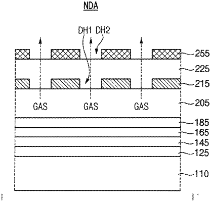
1. A display device, comprising:
a substrate including a display area and a non-display area surrounding at least a portion of the display area;
a first organic insulating layer disposed on the substrate in the non-display area;
a first conductive layer disposed on the first organic insulating layer and including first discharge holes;
a second organic insulating layer disposed on the first conductive layer; and
a transparent conductive layer disposed on the second organic insulating layer and including second discharge holes that substantially entirely line up with the first discharge holes.
|