| CPC H10K 50/822 (2023.02) [H01L 25/167 (2013.01); H01L 25/18 (2013.01); H10K 50/826 (2023.02); H10K 59/13 (2023.02); H10K 59/60 (2023.02); H01L 27/1443 (2013.01); H10K 59/1201 (2023.02); H10K 59/122 (2023.02)] | 16 Claims |

|
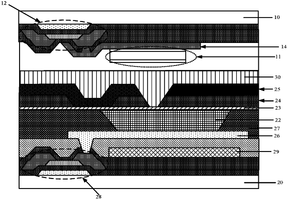
1. A display substrate, comprising a substrate and a plurality of electroluminescent layers on the substrate, wherein
the display substrate further comprises a first reflective electrode layer, a buffer layer and a second reflective electrode layer in direct contact with the buffer layer on a side of at least one of the plurality of electroluminescent layers distal to the substrate;
the buffer layer is provided with a first opening extending along a thickness direction of the buffer layer as a first hollow region, the second reflective electrode layer is provided with a second opening extending along a thickness direction of the second reflective electrode layer as a second hollow region, the first opening is communicated with the second opening, and an overlapping region between the first hollow region and the second hollow region is configured to transmit light emitted by the electroluminescent layer, and
an orthographic projection of the at least one of the plurality of electroluminescent layers on the substrate covers an orthographic projection of the overlapping region on the substrate;
wherein the first reflective electrode layer has a thickness of 200 Å-1000 Å:
wherein a material of the first reflective electrode layer comprises one of ITO-Cs, Li3PO3/Al, MgAg, LiAl, Ca/Ag, Ag/Al, and Ba/Al/ITO; and
wherein an area of the orthographic projection of the overlapping region on the substrate is 5% to 30% of an area of the orthographic projection of the electroluminescent layer on the substrate.
|