| CPC H10K 39/32 (2023.02) [H01L 28/40 (2013.01); H04N 25/75 (2023.01); H01L 27/1463 (2013.01); H01L 27/14621 (2013.01); H01L 27/14627 (2013.01); H01L 27/14636 (2013.01); H01L 27/14643 (2013.01); H01L 27/14689 (2013.01)] | 20 Claims |
|
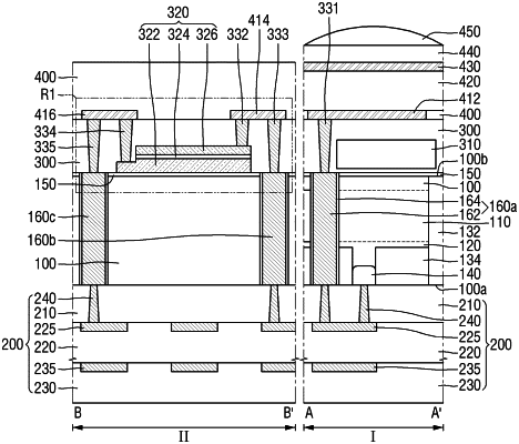
1. An image sensor comprising:
a substrate including a first surface and a second surface, the second surface being opposite the first surface and configured to be light incident;
a photoelectric conversion layer in the substrate,
a wiring structure on the first surface of the substrate, the wiring structure including a plurality of wiring layers;
an interlayer insulating film on the second surface of the substrate;
a capacitor structure in the interlayer insulating film, the capacitor structure including a first conductive pattern, a dielectric pattern, and a second conductive pattern sequentially stacked on the second surface of the substrate;
a first wiring on the interlayer insulating film, the first wiring being connected to one of the first conductive pattern and the second conductive pattern; and
a first penetration via penetrating the substrate and extending from the first surface to the second surface, the first penetration via being connected to the first wiring.
|