| CPC H10B 12/315 (2023.02) [H10B 12/033 (2023.02)] | 20 Claims |
|
1. A semiconductor structure, comprising:
a substrate;
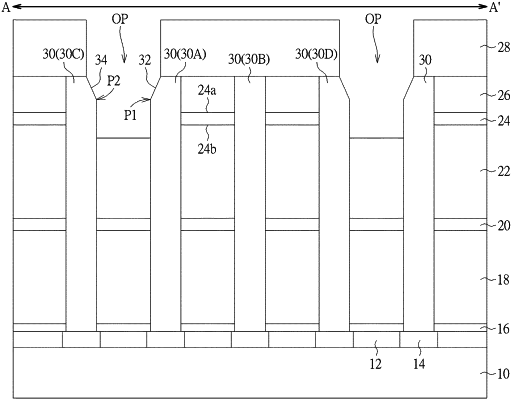
a first bottom electrode and a second bottom electrode disposed on the substrate, wherein the first bottom electrode comprises a first sidewall and a second sidewall, the second bottom electrode comprises a third sidewall and a fourth sidewall, the second sidewall is opposite to the third sidewall, an upper portion of the first sidewall comprises a slope profile;
an upper supporting layer extending laterally between the first bottom electrode and the second bottom electrode and directly contacting the second sidewall and the third sidewall, wherein the upper supporting layer comprises an upper surface and a lower surface, and a lower end of the slope profile of the first sidewall is not lower than the lower surface of the upper supporting layer;
a cavity extending laterally between the substrate and the upper supporting layer;
a capacitor dielectric layer covering along the first bottom electrode and the second bottom electrode; and
a conductive material disposed on the capacitor dielectric layer and filling the cavity.
|