| CPC H10B 12/20 (2023.02) [G11C 5/063 (2013.01); G11C 11/4096 (2013.01); G11C 11/4099 (2013.01); G11C 16/0416 (2013.01); G11C 16/0483 (2013.01); H01L 21/26586 (2013.01); H01L 23/528 (2013.01); H01L 27/0886 (2013.01); H01L 29/1087 (2013.01); H01L 29/1095 (2013.01); H01L 29/66659 (2013.01); H01L 29/785 (2013.01); H01L 29/7841 (2013.01); H10B 12/50 (2023.02); H10B 41/35 (2023.02); H10B 43/35 (2023.02); H10B 69/00 (2023.02); G11C 2211/4016 (2013.01)] | 18 Claims |
|
1. A semiconductor memory array comprising:
a plurality of NAND string configurations, each said NAND string configuration comprising:
a plurality of semiconductor memory cells serially connected to one another to form a string of semiconductor memory cells;
a select gate drain device connected at one end of said string of semiconductor memory cells, wherein said select gate drain device is not a semiconductor memory cell; and
a select gate source device connected at an opposite end from said one end of said string of semiconductor memory cells, wherein said select gate source device is not a semiconductor memory device;
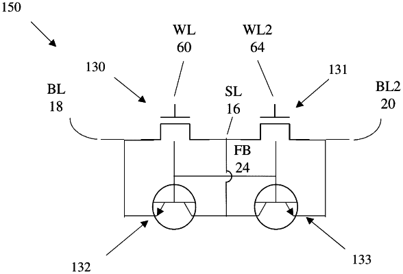
wherein at least one of said plurality of semiconductor memory cells each comprise a substrate and a floating body region formed as part of said substrate and configured to store data as charge therein to define a state of said semiconductor memory cell; a first region in electrical contact with said floating body region; a second region in electrical contact with said floating body region and spaced apart from said first region; and a third region in electrical contact with said floating body region and spaced apart from said first and second regions;
wherein said third region is configured to function as a collector region to maintain a charge of said floating body region, thereby maintaining said state of said floating body region;
wherein said third region is commonly connected to at least two of said semiconductor memory cells;
wherein each said at least one of said plurality of semiconductor memory cells has only one gate;
wherein serial connections between at least two of said semiconductor memory cells are not connected to any terminals;
wherein said select gate drain device is connected to a local bit line; and
at least one transistor isolating said local bit line from a primary bit line.
|