| CPC H10B 12/0335 (2023.02) [H10B 12/315 (2023.02); H10B 12/34 (2023.02); H10B 12/482 (2023.02)] | 17 Claims |
|
1. A method for forming a memory, comprising:
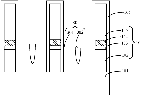
providing a substrate, a plurality of discrete bit line structures being located on the substrate, and an area surrounded by the adjacent bit line structures and the substrate and having a central axis;
forming, on the substrate, a first conductive film filling an area between the adjacent bit line structures;
etching the first conductive film by a first etching process to form a first conductive layer, the thickness of the first conductive layer, in a direction from sidewalls of the bit line structure to the central axis, gradually decreases in a direction perpendicular to the surface of the substrate;
forming a second conductive film on the top surface of the first conductive layer; and
etching the second conductive film and the first conductive layer by a second etching process, the remaining second conductive film and the first conductive layer forming a capacitive contact window, and, by the second etching process, the etching rate for the second conductive film being less than the etching rate for the first conductive layer.
|