|
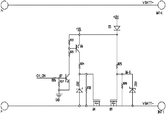
1. An anti-backflow output switch, comprising a switch circuit and a detection circuit, characterized in that the switch circuit comprises a first triode (Q6), a second triode (Q7), a first MOS tube (Q4) and a second MOS tube (Q9), wherein a first resistor (R15) is connected between a base and an emitter of the first triode (Q6), a second resistor (R26) is connected to a base of the second triode (Q7), a third resistor (R27) is connected between a base and an emitter of the second triode (Q7), a collector of the send triode (Q7) is connected to the base of the first triode (Q6) through a fourth resistor (R21), a collector of the first triode (Q6) is connected to a source of the first MOS tube (Q4) through a fifth resistor (R24) and a first diode (ZD2), a sixth resistor (R30) is connected between the source and a gate of the first MOS tube (Q4), the sixth resistor (R30) is connected in parallel with the first diode (ZD2), a drain of the first MOS tube (Q4) is connected to a drain of the second MOS tube (Q9), a gate of the second MOS tube (Q9) is connected to a seventh resistor (R25) and a second diode (D5), an eighth resistor (R28) is connected between the gate and a source of the second MOS tube (Q9), the eighth resistor (R28) is connected in parallel with a third diode (ZD3), the detection circuit comprises a chip (U2) and a third MOS tube (Q10), a drain of the third MOS tube (Q10) is connected to a ninth resistor (R33), a tenth resistor (R37) is connected between a gate and a source of the third MOS tube (Q10), the gate of the third MOS tube (Q10) is connected to a first pin of the chip (U2) through a eleventh resistor (R35), a twelfth resistor (R34) and a thirteenth resistor (R38) are connected to a second pin and a third pin of the chip (U2) respectively, a fourteenth resistor (R39) and a first capacitor (C35) are connected between the first pin and the second pin of the chip (U2), the second pin of the chip (U2) is connected to a fourth pin of the chip (U2) through the first capacitor (C35) and a fourth diode (D7), the model number of the chip (U2) is LM393, and the seventh resistor (R25) is connected to the ninth resistor (R33).
|