| CPC H02M 1/44 (2013.01) [H02M 3/156 (2013.01); H04B 1/69 (2013.01)] | 20 Claims |
|
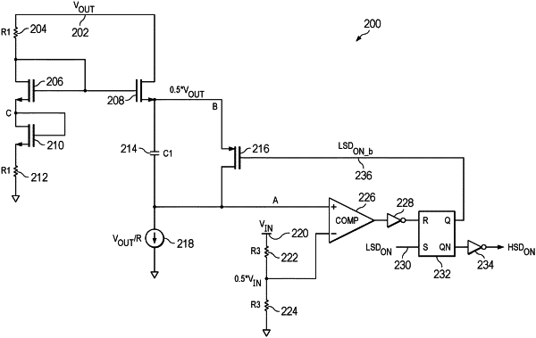
18. A circuit for modulating a drive signal in a switching voltage converter, the circuit comprising:
a first amplifier having first and second amplifier inputs and a first amplifier output;
a first transistor coupled between a first reference voltage terminal and the first amplifier input, and having a first control terminal;
a second transistor coupled between a second reference voltage terminal and the first amplifier input, and having a second control terminal;
a first inverter having a first inverter input and a first inverter output, the first inverter input coupled to the first amplifier output, and the first inverter output coupled to the first control terminal;
a second inverter having a second inverter input and a second inverter output, the second inverter input coupled to the first inverter output, and the second inverter output coupled to the second control terminal;
a second amplifier having third and fourth amplifier inputs and a second amplifier output, the third amplifier input coupled to the second amplifier input;
a third transistor coupled between an output voltage terminal and the fourth amplifier input, and having a third control terminal coupled to the second amplifier output;
a fourth transistor having a current terminal coupled to the output voltage terminal, and having a fourth control terminal coupled to the second amplifier output;
a fifth transistor coupled between the fourth transistor and a ground terminal, and having a fifth control terminal coupled to the fourth transistor;
a comparator having first and second comparator inputs, the first comparator input coupled to a voltage divider; and
a sixth transistor coupled between the ground terminal and the second comparator input.
|