| CPC H01L 31/073 (2013.01) [H01L 31/0296 (2013.01); H01L 31/02966 (2013.01); H01L 31/022441 (2013.01); H01L 31/022466 (2013.01); H01L 31/1828 (2013.01); H01L 31/1832 (2013.01); H01L 31/1864 (2013.01); H01L 31/1884 (2013.01); H01L 31/208 (2013.01)] | 19 Claims |
|
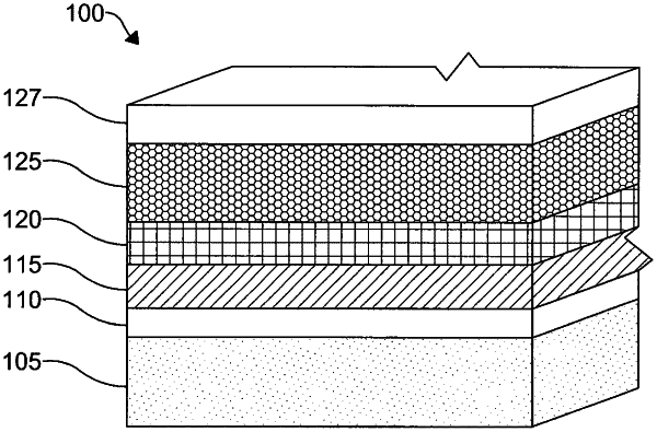
1. A method of forming a photovoltaic device comprising the steps of:
depositing a material comprising CdSe over a TCO layer;
depositing a material comprising CdTe over the material comprising CdSe to form a precursor;
annealing the precursor to form an absorber layer, whereby the material comprising CdSe and at least a portion of the material comprising CdTe interdiffuse to form a CdSeTe alloy;
depositing a material comprising tellurium and zinc, over the absorber layer, to form a back contact over the absorber layer; wherein:
the absorber layer is p-type;
a ratio of Te atoms to a sum of Se atoms and the Te atoms throughout the absorber layer is between about 99 to 100 and about 60 to 100; and
a Se concentration declines across a thickness of the absorber layer toward the back contact.
|