| CPC H01L 29/785 (2013.01) [H01L 27/0688 (2013.01); H01L 27/0924 (2013.01); H01L 29/0847 (2013.01); H01L 29/66795 (2013.01)] | 20 Claims |
|
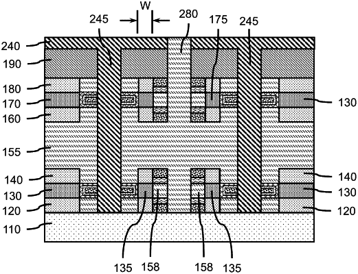
1. A stacked device circuit, comprising:
a first semiconductor layer section on a substrate;
a dielectric fill on the substrate adjoining the first semiconductor layer section;
a second semiconductor layer section on the first semiconductor layer section;
a lower gate structure on the dielectric fill and adjoining the second semiconductor layer section;
a third semiconductor layer section on the second semiconductor layer section; and
an insulating layer on the third semiconductor layer section and lower gate structure.
|