| CPC H01L 29/7827 (2013.01) [H01L 29/063 (2013.01); H01L 29/66666 (2013.01); H01L 29/66818 (2013.01); H01L 29/785 (2013.01)] | 7 Claims |
|
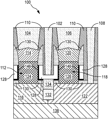
1. A vertical field-effect transistor (VTFET) inverter, comprising:
a p-channel field-effect transistor (P-FET) comprising a P-FET top source/drain (S/D) and a P-FET bottom S/D;
an n-channel field-effect transistor (N-FET) comprising an N-FET top S/D and a N-FET bottom S/D;
a buried contact located at a boundary between the P-FET bottom S/D and the N-FET bottom S/D, wherein an entire top surface of the buried contact is below a top surface of the P-FET bottom S/D and a top surface of the N-FET bottom S/D; and
a Vout contact electrically connected to one of the P-FET bottom source/drain and the N-FET bottom S/D.
|