| CPC H01L 29/2003 (2013.01) [H01L 21/0254 (2013.01); H01L 29/66462 (2013.01); H01L 29/778 (2013.01); H01L 29/78 (2013.01); H01L 29/7786 (2013.01)] | 13 Claims |
|
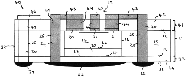
1. A semiconductor device, comprising:
a composite layer having a first surface and a second surface opposing the first surface, the composite layer comprising a mesa and a first insulating layer, the mesa having a top surface, a bottom surface and side faces, the side faces being embedded in the first insulating layer, wherein the mesa comprises a Group III nitride-based multilayer structure that provides a Group III nitride based device having a first electrode and a second electrode that are arranged on the top surface of the mesa, and the first insulating layer is formed of oxide and/or nitride material;
an insulating material positioned on the second surface of the composite layer;
a first outer contact positioned on the insulating material;
a second outer contact positioned on the insulating material;
a first conductive via extending through the first insulating layer and the insulating material, the first conductive via being electrically coupled to the first electrode on the top surface of the mesa and to the first outer contact positioned on the insulating material; and
a second conductive via extending through the first insulating layer and the insulating material, the second conductive via being electrically coupled to the second electrode on the top surface of the mesa and to the second outer contact positioned on the insulating material,
wherein the first outer contact comprises a metallic layer, one or more conductive bumps arranged on the metallic layer, and solder positioned on the conductive bumps.
|