| CPC H01L 29/0607 (2013.01) [H01L 29/41708 (2013.01); H01L 29/42304 (2013.01)] | 14 Claims |
|
1. A semiconductor device, comprising:
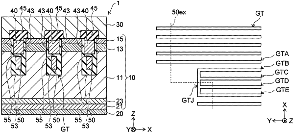
a semiconductor layer having a first surface in which a plurality of trenches each extending along a first surface direction are arranged along a second surface direction perpendicular to the first surface direction;
a first electrode on a second surface of the semiconductor layer;
a second electrode on the first surface of the semiconductor layer;
a control electrode inside one or more of the trenches;
a third electrode inside each of the trenches, the control electrode being inside each of the trenches between the second and third electrodes;
a first wiring extending along the second surface direction above the first surface of the semiconductor layer at an end in the first surface direction of each of the trenches, and electrically connected to the second electrode and the third electrode in each of the trenches; and
a first contact provided between the semiconductor layer and the first wiring, the first wiring and the third electrode in two or more of the trenches being electrically connected via the first contact, wherein
the plurality of trenches includes first, second, and third trenches,
the first and second trenches are connected to each other via a first connector trench that is provided at an end in the first surface direction of each of the first and second trenches and extends in the second surface direction, and
the third trench extends beyond the end of each of the first and second trenches along the first surface direction.
|