| CPC H01L 27/1288 (2013.01) [H01L 27/1248 (2013.01); H01L 29/41733 (2013.01); H01L 27/1225 (2013.01)] | 13 Claims |
|
1. A thin film transistor, comprising:
a gate electrode;
an active layer disposed corresponding to the gate electrode;
a source electrode;
a drain electrode, wherein the source electrode and the drain electrode are disposed at both sides of the active layer and electrically connected to the active layer; and
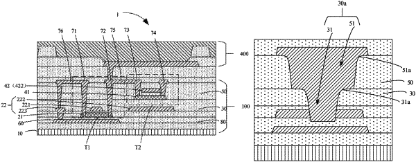
an interlayer insulating layer disposed between the active layer and the source electrode, and between the active layer and the drain electrode, wherein the interlayer insulating layer is provided with step-shaped contact holes, and the source electrode and the drain electrode are filled in the contact holes and electrically connected to the active layer;
wherein each of the contact holes is composed of a first contact hole and a second contact hole that communicate with each other, the first contact hole is disposed on a side of the second contact hole away from the active layer, a diameter of the first contact hole is greater than that of the second contact hole, the first contact hole has a first smooth rounded surface at its end away from the active layer, and the second contact hole has a second smooth rounded surface at its end away from the active layer.
|