| CPC H01L 27/124 (2013.01) [H01L 24/03 (2013.01); H01L 24/05 (2013.01); H01L 25/167 (2013.01); H01L 27/1262 (2013.01); H01L 27/1288 (2013.01); H01L 2224/03622 (2013.01); H01L 2224/03825 (2013.01); H01L 2224/05022 (2013.01); H01L 2224/05073 (2013.01); H01L 2224/05147 (2013.01); H01L 2224/05562 (2013.01); H01L 2224/05573 (2013.01); H01L 2224/05611 (2013.01)] | 12 Claims |
|
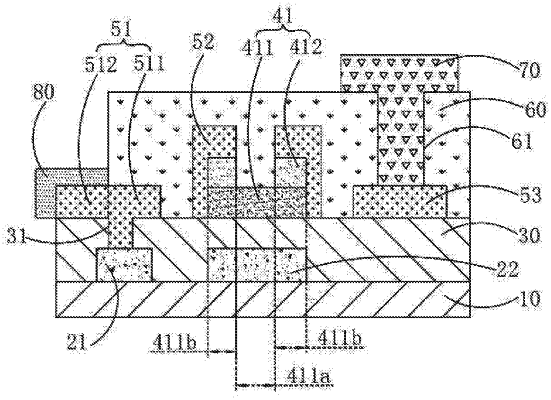
1. A light-emitting panel, comprising: a light-emitting board, the light-emitting board including a light-emitting area and a bonding area located beside the light-emitting area, wherein the light-emitting board includes:
a substrate;
a first metal layer disposed on the substrate and comprising a gate and a scanning line electrically connected to the gate;
a gate insulating layer covering the first metal layer and comprising a connection hole defined through the gate insulating layer;
a second metal layer disposed on a side of the gate insulating layer away from the first metal layer; and
a light-emitting chip disposed on a side of the second metal layer away from the gate insulating layer;
wherein the second metal layer includes a chip-scanning-line connection portion located in the bonding area and electrically connected to the scanning line through the connection hole, and a conductive protection layer formed by chemical plating is disposed on a surface of the chip-scanning-line connection portion.
|