| CPC H01L 27/0629 (2013.01) [H01L 21/0217 (2013.01); H01L 21/0254 (2013.01); H01L 21/0262 (2013.01); H01L 21/02164 (2013.01); H01L 21/02381 (2013.01); H01L 21/02458 (2013.01); H01L 21/26513 (2013.01); H01L 21/26586 (2013.01); H01L 21/28556 (2013.01); H01L 21/28575 (2013.01); H01L 21/30612 (2013.01); H01L 21/8258 (2013.01); H01L 29/16 (2013.01); H01L 29/2003 (2013.01); H01L 29/205 (2013.01); H01L 29/66128 (2013.01); H01L 29/66136 (2013.01); H01L 29/66462 (2013.01); H01L 29/7786 (2013.01); H01L 29/8611 (2013.01)] | 18 Claims |
|
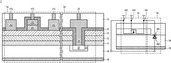
1. A GaN-based semiconductor device, comprising:
a doped substrate;
a barrier layer, disposed on the doped substrate;
a channel layer, disposed between the doped substrate and the barrier layer;
a source, gate, and drain formed on an upper surface of the barrier layer;
a doped semiconductor structure, disposed in the doped substrate, wherein
a band gap of the barrier layer is greater than a band gap of the channel layer with a two-dimensional electron gas formed in the channel layer;
the doped substrate and the doped semiconductor structure disposed in the doped substrate have different polarities to form a diode;
a conductive structure formed adjacent to the drain, and laterally spaced from the drain and positioned on an upper surface of an insulation layer positioned on the upper surface of the barrier layer and having a conductive portion extending through an aperture in the barrier layer and the channel layer to form an ohmic contact with the diode; and
the insulating layer positioned on the upper surface of the barrier layer further extending into the aperture in the barrier layer and the channel layer and lining a sidewall of the aperture in the barrier layer and the channel layer;
wherein
the drain is electrically connected to the doped semiconductor structure; and
the source is electrically connected to the doped substrate, and
the drain is electrically connected to a cathode of the diode, and
the source is electrically connected to an anode of the diode.
|