| CPC H01L 25/18 (2013.01) [H01L 23/5226 (2013.01); H01L 23/5283 (2013.01); H01L 24/08 (2013.01); H01L 24/16 (2013.01); H01L 24/32 (2013.01); H01L 23/53223 (2013.01); H01L 23/53238 (2013.01); H01L 23/53266 (2013.01); H01L 2224/08145 (2013.01); H01L 2224/08501 (2013.01); H01L 2224/16145 (2013.01); H01L 2224/32145 (2013.01); H01L 2224/32501 (2013.01); H01L 2924/01006 (2013.01); H01L 2924/01007 (2013.01); H01L 2924/01014 (2013.01)] | 45 Claims |
|
1. An integrated circuit (IC) package, comprising:
an IC component having a first face and an opposing second face; and
a microelectronic assembly, coupled to the IC component by IC component interconnects, the microelectronic assembly comprising:
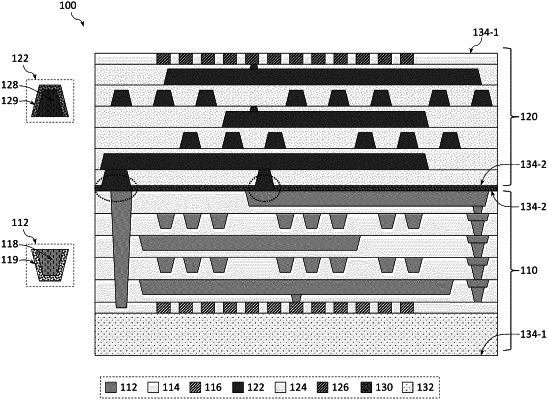
a first IC structure having a first face and an opposing second face, wherein the first face of the first IC structure is at least partially between the second face of the IC component and the second face of the first IC structure, and the first face of the first IC structure is coupled to the second face of the IC component by the IC component interconnects,
a second IC structure having a first face and an opposing second face, wherein the first face of the second IC structure is at least partially between the second face of the first IC structure and the second face of the second IC structure,
a bonding interface between the second face of the first IC structure and the first face of the second IC structure, and
a plurality of vias, wherein an individual via includes an electrically conductive material, has a portion in the first IC structure and a portion in the second IC structure, and extends through the bonding interface, and wherein a pitch of the plurality of vias is different from a pitch of the IC component interconnects.
|