| CPC H01L 21/7681 (2013.01) [H01L 21/31116 (2013.01); H01L 21/31144 (2013.01); H01L 21/76877 (2013.01)] | 20 Claims |
|
1. A method for forming a hole structure in a semiconductor device using a single photolithography process, comprising:
forming an etch mask having a hard mask layer and a photoresist layer, wherein the hard mask layer is formed directly on a stack structure and the photoresist layer is formed on the hard mask layer, the stack structure including a plurality of sublayers stacked above an etch stop layer;
patterning the photoresist layer using the single photolithography process to form a first pattern over the hard mask layer; and
removing portions of the hard mask layer exposed by the first pattern of the photoresist layer, such that remaining portions of the hard mask layer and the photoresist layer form the etch mask having a mask opening with a first lateral dimension;
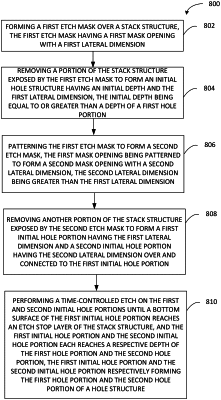
removing a portion of the stack structure exposed by the mask opening to form an initial hole structure, the initial hole structure partially through an intermediate one of the plurality of sublayers of the stack structure without exposing or penetrating the etch stop layer of the stack structure;
after forming the initial hole structure, enlarging the mask opening of the etch mask, including using an oxygen plasma etching process to form a second pattern in the photoresist layer and removing portions of the hard mask layer exposed by the second pattern of the photoresist layer to form an enlarged mask opening in the etch mask, the enlarged mask opening having a second lateral dimension that is greater than the first lateral dimension; and
removing an other portion of the stack structure exposed by the enlarged mask opening to form the hole structure from the initial hole structure, the hole structure having a first hole portion and a second hole portion connected to and over the first hole portion, a bottom of the hole structure exposing the etch stop layer.
|