| CPC H01L 21/268 (2013.01) [H01L 21/6835 (2013.01); H01L 25/0657 (2013.01)] | 7 Claims |
|
1. A laminated element manufacturing method comprising:
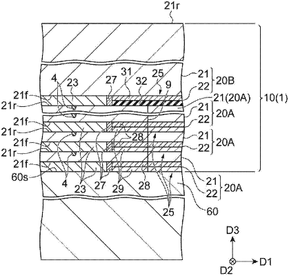
a preparing step of preparing a first wafer, a second wafer, and a third wafer, each of the first wafer, the second wafer, and the third wafer including a semiconductor substrate having a front surface and a back surface, and a circuit layer including a plurality of functional elements two-dimensionally arranged along the front surface;
a first bonding step of bonding the circuit layer of the first wafer to the circuit layer of the third wafer such that each of the functional elements of the third wafer correspond to each of the functional elements of the first wafer;
a first forming step of forming a first modified region along a line to cut by irradiating the semiconductor substrate of the first wafer with a laser light along the line to cut set to pass between each of the functional elements, after the first bonding step;
a first grinding step of grinding the semiconductor substrate of the first wafer after the first forming step;
a second bonding step of bonding the circuit layer of the second wafer to the semiconductor substrate of the first wafer such that each of the functional elements of the first wafer correspond to each of the functional elements of the second wafer, after the first grinding step;
a second forming step of forming a second modified region along the line to cut by irradiating the semiconductor substrate of the second wafer with a laser light along the line to cut, after the second bonding step;
a second grinding step of grinding the semiconductor substrate of the second wafer after the second forming step;
a third forming step of forming a third modified region along the line to cut by irradiating the semiconductor substrate of the third wafer with a laser light along the line to cut, after the second grinding step; and
a third grinding step of grinding the semiconductor substrate of the third wafer after the third forming step.
|