| CPC H01J 37/32082 (2013.01) [C23C 16/4411 (2013.01); C23C 16/4412 (2013.01); C23C 16/45565 (2013.01); C23C 16/505 (2013.01); C23C 16/5096 (2013.01); H01J 37/3244 (2013.01); H01J 37/32091 (2013.01); H01J 37/32458 (2013.01); H01J 37/32467 (2013.01); H01J 37/32568 (2013.01); H01J 37/32577 (2013.01); H10K 71/00 (2023.02); C23C 16/345 (2013.01); H01J 2237/3321 (2013.01); H10K 71/164 (2023.02)] | 10 Claims |
|
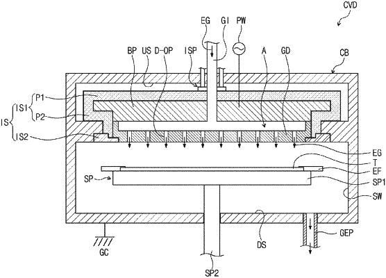
1. A method of manufacturing a display apparatus, the method comprising:
preparing a substrate having an organic light-emitting diode on a susceptor disposed in a chamber;
forming a plasma region disposed over the susceptor by applying power to a backing plate of which a top surface and a sidewall are covered by an insulator; and
providing a deposition gas into the plasma region to form a first inorganic thin layer on the organic light-emitting diode,
wherein the insulator including:
a first portion covering the top surface of the backing plate, the first portion including a plurality of protrusions which protrude from edges of the first portion toward the backing plate to cover sides of the backing plate; and
a second portion assembled with the first portion and covering a sidewall of the backing plate, the second portion including a plurality of engaging portions which are recessed from a top surface of the second portion and are disposed in regions corresponding to the plurality of protrusion, and
wherein the plurality of protrusions in the first portion and the plurality of engaging portions in the second portion are coupled to each other to receive the backing plate in a space formed by the first portion and the second portion.
|