| CPC G11C 19/184 (2013.01) [G09G 3/3225 (2013.01); G11C 19/188 (2013.01); H01L 27/124 (2013.01); H01L 27/1225 (2013.01); H01L 27/1255 (2013.01); G09G 2310/0286 (2013.01); G09G 2320/02 (2013.01); G09G 2330/021 (2013.01)] | 17 Claims |
|
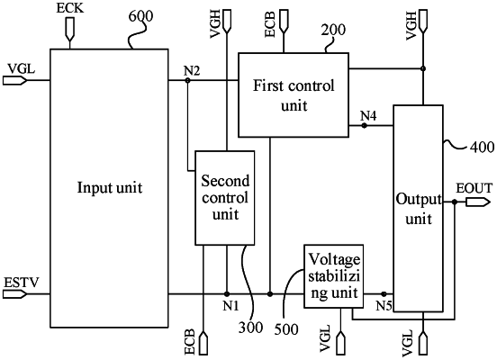
1. A shift register, comprising: an input unit, a first control unit, a second control unit, an output unit, and a voltage stabilizing unit,
wherein the input unit is respectively connected to a signal input end, a first power supply end, a first clock signal end, a first node, and a second node, and is configured to provide a signal of the signal input end to the first node and provide a signal of the first power supply end to the second node under control of the first clock signal end;
the first control unit is respectively connected to the first node, the second node, a fourth node, a second power supply end, and a second clock signal end, and is configured to control a signal of the fourth node according to the signals of the first node and the second node;
the second control unit is respectively connected to the first node, the second node, the second power supply end, and the second clock signal end, and is configured to provide a signal of the second power supply end to the first node under control of the second node and the second clock signal end;
the output unit is respectively connected to the fourth node, a fifth node, the first power supply end, the second power supply end, and an output end, and is configured to provide the signal of the second power supply end or the first power supply end to the output end under control of the fourth node and the fifth node; and
the voltage stabilizing unit is respectively connected to the first node, the fifth node, the output end, and the first power supply end, and is configured to keep the signal of the output end stable when the output unit provides the signal of the first power supply end to the output end;
wherein the input unit is connected to the first control unit and the second control unit through the first node and the second node;
the first control unit is connected to the second control unit through the first node and the second node, and connected to the output unit through the fourth node;
the voltage stabilizing unit is connected to the input unit, the first control unit and the second control unit through the first node, connected to the output unit through the fifth node, and connected to the output end of the output unit.
|