| CPC G11C 16/16 (2013.01) [G11C 16/0433 (2013.01); G11C 16/08 (2013.01); G11C 16/24 (2013.01); G11C 16/26 (2013.01)] | 18 Claims |
|
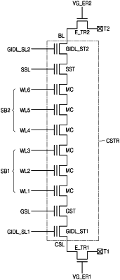
1. A memory device comprising:
a memory block comprising a first sub-block and a second sub-block that are connected between a common source line and a plurality of bit lines and vertically stacked; and
a control circuit configured to select any one of the common source line and the plurality of bit lines as a transmission path of an erase voltage based on positions of the first sub-block and the second sub-block, and perform erase operations on the first sub-block and the second sub-block in units of sub-blocks,
wherein the memory block further comprises:
a first erase transistor directly connected to the common source line, and configured to apply the erase voltage to the common source line; and
a second erase transistor directly connected to the plurality of bit lines, and configured to apply the erase voltage to the plurality of bit lines.
|