| CPC G11C 11/419 (2013.01) [G11C 11/412 (2013.01)] | 17 Claims |
|
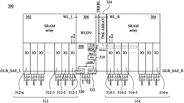
1. A memory device, comprising:
a plurality of memory arrays including a first memory array and a second memory array;
a controller including a plurality of buffers including a first buffer connected to the first memory array and a second buffer connected to the second memory array, wherein the first and second memory arrays are disposed on opposing sides of the controller;
a reset clock generator configured to generate a first signal;
a sense amplifier enable (SAE) generator configured to generate a second signal based on the first signal; and
a plurality of interconnect structures including:
a first interconnect structure extending in a first direction and connected to the first buffer;
a second interconnect structure extending in the first direction and connected to the second buffer, wherein the first and second interconnect structures are disposed in a first metal layer, and wherein the reset clock generator and the SAE generator are interposed between the first buffer and the second buffer; and
a third interconnect structure connected to the first and second interconnect structures and extending in a second direction that is substantially perpendicular to the first direction, wherein the third interconnect structure, disposed in a second metal layer, is electrically connected to the controller,
wherein respective lengths of the first interconnect structure and the second interconnect structure are substantially the same.
|