| CPC G06F 3/0655 (2013.01) [G06F 3/0604 (2013.01); G06F 3/0679 (2013.01)] | 14 Claims |
|
1. A write operation circuit applied to a semiconductor memory, the write operation circuit comprising:
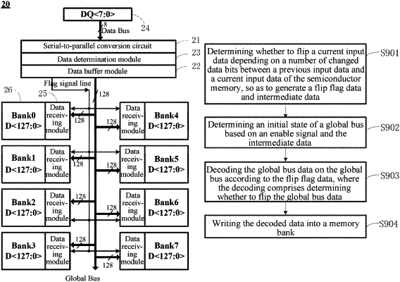
a data determination module, configured to determine whether to flip a current input data of the semiconductor memory depending on a number of changed data bits between a previous input data and the current input data of the semiconductor memory to generate a flip flag data and an intermediate data;
a data buffer module, coupled to the data determination module and configured to determine an initial state of a global bus based on an enable signal and the intermediate data; and
a data receiving module coupled to a memory bank, wherein the data receiving module is configured to receive a global bus data on the global bus, receive the flip flag data through a flip flag signal line, decode the global bus data according to the flip flag data, and write a decoded data into the memory bank of the semiconductor memory, wherein the decoding comprises determining whether to flip the global bus data.
|